
Abstract
Fraunhofer IISB offers prototyping services for electron devices. Such prototyping builds on proven processes and designs, amending them with customer-specific specifications and additions. The challenge is to efficiently combine existing expertise and proven process/device modules with “on the fly” R&D results and novel findings. In this paper, we present a first solution approach for a smart platform for rapid prototyping in order to improve time-to-market in low-volume device fabrication. This solution covers research of a digital twin for optimized management of wafer containers, development of intelligent algorithms for process and equipment control as well as a novel approach for “smart experiments” to achieve an accelerated transfer of process development to ISO-certified production.
You have full access to this open access chapter, Download conference paper PDF
Keywords
1 Motivation
The Fraunhofer IISB runs the π-Fab (see Fig. 1), which comprises a continuous silicon CMOS process line in an industry-compatible environment, completed with specific equipment for processing of silicon carbide. Here, prototyping services for electron devices (i.e., power devices, CMOS devices, passives, sensors and MEMS) and processes are offered and performed.

Fraunhofer IISB’s π-Fab covers R&D and ISO-certified rapid prototyping of semiconductor devices. Customers may transfer results from rapid prototyping to mass manufacturing at other sites.
The main challenge for such a prototyping line is to address a multitude of customer requirements in a flexible manner, e.g., with regard to material, device layout, or functionality. While most custom designs build and rely on a proven and optimized set of process steps, it is the mere nature of “prototyping” to replace or augment existing process steps with novel or modified ones, which are tailored to the respective customer’s needs. This requires the smart combination of a certified library of proven process or device modules with results from “on the fly” research and development. As any low-volume production site with high product diversity, the π-Fab faces the challenge of an ever-changing product-specific knowledge base. Maintaining such a flexible environment requires effective learning and implementation strategies in order to achieve highest quality and repeatability for the customers. Such a smart, effective and flexible platform for prototype device fabrication has to consider knowledge management, smart experiments (Davenport 2009), digital twins, smart logistics (Sturm 2006) and smart organization.
2 New Concepts for Manufacturing Control and Fast Process Transfer
To achieve substantial progress in these areas, Fraunhofer IISB carries out focused research and development within the European project iDev4.0 (“integrated Development 4.0”) to evolve its π-Fab towards a smart platform for rapid prototyping. The research approach is to elaborate, and in the long run to implement, a digital duplication of the π-Fab (see Fig. 2).

The digital twin of Fraunhofer IISB’s π-Fab collects data, extracts information from it and turns the obtained information into knowledge and actions.
The concept of using such a digital copy of the physical system to perform real-time optimization is often referred to as a “digital twin” (Söderberg 2017): The digital twin can be used to collect and store data and information from the real world, learn from it and turn the results into knowledge and actions for the real world again.
The first step towards the “π-Fab digital twin” will focus on smart experiments for accelerated process transfer and flexible concepts for manufacturing control, tailored to a rapid prototyping environment. Respective results will be used to augment existing π-Fab elements in a smart manner to enable new perspectives for the prototype fabrication of small lot-sizes with high product diversity on different substrate materials.
Thus, R&D effort of Fraunhofer IISB and collaboration with project partners in iDev4.0 focuses on three areas:
-
1.
Virtual Factory Cluster:
-
Research of a local digital twin for an optimized management of wafer containers in a combined development and manufacturing environment. This digital twin will later become a part of the overarching “π-Fab digital twin”.
-
Development of intelligent algorithms for process and equipment control in a rapid prototyping environment.
-
-
2.
Smart Experiments: Research of a novel approach for “Smart Experiments” to achieve an accelerated transfer from process development to ISO-certified production.
-
3.
Real Time Control and Planning 4.0: Elaboration of flexible concepts for manufacturing control, tailored to a rapid prototyping environment.
Respective results will be used to augment existing π-Fab elements in a smart manner to enable new perspectives for the prototype fabrication of small lot-sizes with high product diversity on different substrate materials (see Fig. 3).

First solution approach to evolve the π-Fab towards a smart platform for rapid prototyping
3 Results
Within the first period of the iDev4.0 project, several steps have been taken to realize the above described solution approach. Specific focus was on smart logistics and contamination control (area 1 and 3) and smart experiments (area 2).
3.1 Smart Experiments
In the flexible prototyping environment of the π-Fab with a wide mix of products, low product volumes as well as both R&D and production evolving in parallel in the same manufacturing line, an efficient use of any available bit of information and data is essential to quickly transfer latest R&D results into certified prototyping. To achieve this objective, we started research on the novel concept of “smart experiments”. So far, two important steps were taken:
-
1.
A group of experts from the equipment, process and data analytics domains identified in a joint effort the most challenging processes that require accelerated process transfer. As a result, the focus will be on an etch cluster tool, comprising three chambers dedicated to specific etching steps.
-
2.
In parallel, a concept for smart experiments was developed. Figure 4 summarizes the initial concept, while the alignment of the approach with the other project partners is ongoing.
Fig. 4. 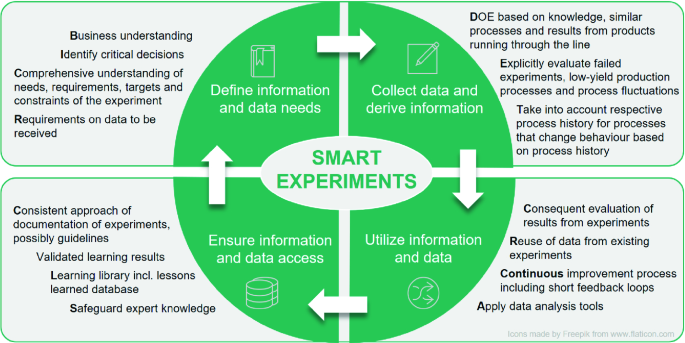
The concept of “smart experiments”.

By applying this approach, a quick identification of a high quality and comprehensive set of experiments is aimed for, resulting in a decrease of design and learning cycle time. The first concept evaluation and validation approach considering dry etch processes will show, whether the aspired 20% reduction of integration-time for newly developed processes becomes possible.
3.2 Smart Logistics and Flexible Manufacturing Control for Rapid Prototyping
For high quality and reliable products, it is common in industrial high volume production to use only precisely defined processes and to monitor the processes closely by means of various software systems, such as a manufacturing execution system (MES). This is a distinct difference to Fraunhofer IISB’s prototype fabrication of electron devices, where a multitude of customer requirements with regard to material, device layout, or functionality is being addressed in the process pool. This flexibility is a matter of principle and leads to continuous variations of process steps and process flows in the prototype fabrication. In order to optimize the entire value chain, from order to customer and back again for process/device improvements, flexible manufacturing control techniques have to be developed and applied.
Fraunhofer IISB is working within iDev4.0 on smart logistics and flexible manufacturing control concepts for rapid prototyping. Functionalities and requirements for adaptive process flow planning, process execution and process parameter adjustment based on results of real-time and smart experiments are currently being defined. The developed concepts will be later implemented in the new manufacturing execution system, which will be rolled out as part of the “Research Fab Microelectronics Germany/Forschungsfabrik Mikroelektronik Deutschland (FMD)”.
Another important challenge in manufacturing and prototyping, respectively, is the implementation of smart logistics for wafer carriers. Based on the π-Fab’s flexibility, various wafer sizes and types are being handled in different contamination protocol zones and the customer may determine the points of entry and exit in the process line. To overcome this challenge, innovative carrier monitoring strategies are currently developed by Fraunhofer IISB utilizing the concept of digital twins. During the project, a prototype for the data-driven contamination monitoring of FOUPs in the production line at Infineon will be developed. All the techniques learned reaching from the analysis equipment to the different contamination sources in a power semiconductor fab to data management of carrier data will be taken into account when implementing an optimized wafer container monitoring in the Pi-Fab. This could be for example the introduction of carrier changes or adding time coupling after certain steps.
Figure 5 shows the principle of the intended concept for a digital twin of a wafer container. The tracking information of the wafer and the corresponding wafer container will be combined with the analysis of data from in-line and off-line contamination control procedures to improve carrier logistics with regard to contamination. First investigations have been started with data sets provided by an industrial project partner.

Digital twin principle for wafer container
4 Summary
A first solution approach towards a smart platform for rapid prototyping of low-volume devices was outlined and actual implementation started. The approach comprises R&D in smart experiments, digital twins, smart logistics and smart organization. The actual development of solutions was preceded by a survey. This procedure is in line with the proven approach described, e.g., by the CRISP-DM model (Shearer 2000): This step is focused on knowledge and understanding of the objective on the one hand, and the alignment of expectations of the stakeholders on the other. Similarly, McKinsey describes an “advanced analytics” approach, which they suggest to apply in semiconductor industry in general and R&D in particular. In contrast to traditional analytics, they also recommend to start from the business problem that needs to be solved and to head for information and respective data needed to derive the correct decisions in respect thereof (Batra 2016).
Project Information:
The project “integrated Development 4.0” leads the digital transformation of singular processes towards an integrated digital value chain based on the “digital twin” concept. Development, planning and manufacturing will benefit from the “digital twin” concept in terms of highly digitized virtual processes along the whole product lifecycle.
The project iDev4.0 has received funding from the ECSEL Joint Undertaking under grant agreement No 783163. The JU receives support from the European Union’s Horizon 2020 research and innovation program. It is co-funded by the consortium members, grants from Austria, Germany, Belgium, Italy, Spain and Romania.
References
Batra, G.: Improving the semiconductor industry through advanced analytics. McKinsey & Company. Website, March 2016 (2016). https://www.mckinsey.com/industries/semiconductors/our-insights/improving-the-semiconductor-industry-through-advanced-analytics. Accessed 05 Oct 2018
Davenport, T.H.: How to design smart business experiments. Strateg. Dir. 25(8) (2009). https://doi.org/10.1108/sd.2009.05625had.004
Shearer, C.: The CRISP-DM model: the new blueprint for data mining. J. Data Warehous. 5(4), 13–32 (2000)
Söderberg, R.: Toward a digital twin for real-time geometry assurance in individualized production. CIRP Ann. 66(1), 137–140 (2017)
Sturm, R.: Model-based approach for online performance evaluation of automated transportation systems in semiconductor manufacturing. Universität Stuttgart (2006). https://doi.org/10.18419/opus-4090
Author information
Authors and Affiliations
Corresponding author
Editor information
Editors and Affiliations
Rights and permissions
Open Access This chapter is licensed under the terms of the Creative Commons Attribution 4.0 International License (http://creativecommons.org/licenses/by/4.0/), which permits use, sharing, adaptation, distribution and reproduction in any medium or format, as long as you give appropriate credit to the original author(s) and the source, provide a link to the Creative Commons license and indicate if changes were made.
The images or other third party material in this chapter are included in the chapter's Creative Commons license, unless indicated otherwise in a credit line to the material. If material is not included in the chapter's Creative Commons license and your intended use is not permitted by statutory regulation or exceeds the permitted use, you will need to obtain permission directly from the copyright holder.
Copyright information
© 2020 The Author(s)
About this paper

Cite this paper
Schellenberger, M., Anger, S., Pfeffer, M., Häublein, V., Roeder, G., Bauer, A. (2020). Smart Platform for Rapid Prototyping: A First Solution Approach to Improve Time-to-Market and Process Control in Low-Volume Device Fabrication. In: Keil, S., Lasch, R., Lindner, F., Lohmer, J. (eds) Digital Transformation in Semiconductor Manufacturing. EADTC EADTC 2018 2019. Lecture Notes in Electrical Engineering, vol 670. Springer, Cham. https://doi.org/10.1007/978-3-030-48602-0_12
Download citation
DOI: https://doi.org/10.1007/978-3-030-48602-0_12
Published:
Publisher Name: Springer, Cham
Print ISBN: 978-3-030-48601-3
Online ISBN: 978-3-030-48602-0
eBook Packages: EngineeringEngineering (R0)