
Abstract
We report the growth mechanism of metal oxide nanostructures synthesized by electron beam evaporation. The condensed electron beam can easily decompose metal oxide sources that have a high melting point, thereby creating a self-catalytic metal nanodot for the vapor-liquid-solid process. The metal oxide nanostructures can be grown at a temperature just above the melting point of the self-catalyst by dissolving oxygen. The morphology of nanostructures, such as density and uniformity, strongly depends on the surface energy and surface migration energy of the substrate. The density of the self-catalytic metal nanodots increased with decreasing surface energies of the substrate due to the perfect wetting phenomenon of the catalytic materials on the high surface energy substrate. However, the surfaces with extremely low surface energy had difficulty producing the high density of self-catalyst nanodot, due to positive line tension, which increases the contact angle to >180°. Moreover, substrates with low surface migration energy, such as single layer graphene, make nanodots agglomerate to produce a less-uniform distribution compared to those produced on multi-layer graphene with high surface migration energy.
Introduction
One-dimensional metal oxide nanostructures have great potential in a huge number of application fields, including energy and environmental science, electronics, photonics and biology1,2,3,4,5. The growth mechanism of the metal oxide nanostructures can mainly be divided into two categories, based on whether or not metallic catalysts are used6,7,8. The vapor-liquid-solid (VLS) growth mode uses nano-sized metal dots (e.g., Au, Ni) at the early stage of growth and the immersed supersaturated atoms during growth, segregated as the metal oxide nanostructures near the melting point of the catalyst metal. On the other hand, the vapor-solid (VS) growth mode is strongly affected by the anisotropic properties between crystal orientations of nano-sized oxide seed particles, resulting in the facile synthesis of nanostructures. Compared to the VS mode, the VLS mode has the advantages of i) freedom of oxide material selection, ii) a simple process for the nanostructure growth at temperature just above the melting point of the metal catalyst.
A drawback of the VLS process is that, the metal catalyst can react with the target materials during growth at high temperatures, thereby creating intermetallic compounds and contamination9,10. Therefore, VLS that uses the metal element of the target metal oxide as a catalyst (i.e., self-catalyst) has been attempted by decomposing the metal oxide during growth for formation of high quality products without contamination11,12,13,14. However, the decomposition temperature of most metal oxides is too high to control. Carbo-thermal decomposition, in which graphite powder is mixed with the metal oxide powder, can be used to reduce the decomposition temperature, but this process also has contamination problems, such as metal carbide formation13,14. Alternatively, use of an electron beam can decompose several materials that have a high melting point. Several groups have attempted electron beam evaporation to grow nanowires such as Si, Ge and SnO215,16,17. In most of the studies, an Au nanodot was used as the catalyst during VLS. Catalysts that have low melting points, such as In and Bi, have been used to reduce the growth temperatures, but they are heterogeneous catalysts18,19. For the case of metal oxides, heterogeneous catalysts are not needed if the metal element of the metal oxide can be used by decomposing it during growth. Moreover, the decomposition temperature of metal oxide can be reduced under conditions of low oxygen chemical potential, such as in a high vacuum20. Most metal oxides can be easily decomposed by the condensed electron-beam and sufficient metal flux for the self-catalyst of the VLS process can be formed under a low oxygen partial pressure. In this case, the VLS growth can be achieved easily, at a temperature just above the melting point of the metallic self-catalyst, as shown in Fig. 1. The electron beam can easily achieve the vapor pressure required for self-catalyst formation, compared to the conventional tools for nano-structure growth, such as a heat furnace and pulsed laser. Because the maximum temperature of a normal heat furnace is <1,500°C, it has limited application for metal oxides with decomposition temperatures > 1,500°C. Moreover, the pulsed laser tool tends to form the stoichiometrically identical composition to the target source material during laser irradiation, without decomposing of the metal oxide. Overall, the electron beam evaporation is the most ideal tool for nanowire growth using self-catalysis by decomposing of the metal oxide during irradiation.

Schematics of the electron beam evaporation model for metal oxide nanowire growth and growth mechanism by VLS.
In this work, we focused on the group 13 elements in the periodic table (Al, Ga and In) that have high decomposition temperatures for their metal oxides, but, low melting points of metals themselves, as shown in Fig. 2a (Refer to supplementary information S1 for the growth of MgO nanowire by electron beam evaporation using MgO pellet as a source material without use of a catalyst). By checking the morphological changes at temperature below and above the melting point of the metal, self-catalytic VLS of electron beam-evaporated group 13 oxides can be verified. To learn the growth mechanism of liquid metal mediated VLS growth for the metal oxide nanostructures, the effect of surface energy on the nucleation of the self-catalytic nanodots was examined. Although high surface energy is helpful for conventional heterogeneous nucleation, it does not form a nano-sized droplet, but tends to spread easily, resulting in low density of nanostructures21. Finally, the effect of surface migration energy on the nucleation of the self-catalytic nanodots for the VLS process was studied using an n-graphene layer as the substrate, because the surface energy of n-graphene is independent of n, whereas the surface migration energy is strongly dependent on it22,23,24.

(a) Melting point of group 13 elements (pure metal and metal oxide). (b) Top view SEM images of electron beam-evaporated group 13 oxide materials on SiO2 covered Si (100) wafer at RT and near the melting point of the pure 13 group metals. Scale bar, 500 nm. TEM-EELS maps (oxygen, metal element: gallium and indium) and color contour maps of electron beam evaporated (c) gallium oxide and (d) indium(tin) oxide on Si (100) substrate at the early stage of growth.
Results and Discussion
SEM images (Fig. 2b) were taken of electron beam-evaporated group 13 oxide materials on SiO2 covered Si (100) wafers at room temperature (RT) and near melting point of the pure metals (Al: 660.03°C, Ga: 29.77°C and In: 156.6°C). The surface morphologies of the samples were quite flat at RT, except for Ga2O3, whereas there were several nanostructures near the melting point of the pure metal. The rough surface of Ga2O3 at RT resulted from the low melting point of pure Ga and the even lower melting point of the nano-sized dot than the bulk state; as a result, the liquid phase occurred during deposition even at RT25,26. These metal oxides could be decomposed easily by a high density electron-beam and sufficient metal flux for self-catalysis of the VLS process can be formed under a low oxygen partial pressure. In this case, VLS growth can be achieved easily at a temperature just above the melting point of the metallic self-catalyst, resulting in development of nanostructures. To verify that self-catalytic VLS growth occurs, the most important is the existence of metallic nanodots at the early stages of growth.
Figure 2c and 2d show the electron energy loss spectroscopy in a transmission electron microscope (TEM-EELS) maps of electron beam-evaporated gallium oxide and indium(tin) oxide (ITO) exposed for just for 10 sec on Si (100) substrate at 100°C for gallium oxide and 300°C for indium(tin) oxide. To protect against oxidation during transfer from the electron beam evaporator to the TEM, each sample was passivated in-situ using an amorphous SiO2 layer (~70 nm thick). In the maps, oxygen and the metal element were separated by a clear line, which clearly proves the existence of metallic nanodots at the initial stage of nanostructure growth. Based on this clue about metallic nanodot formation, we can study the growth mechanism of these nanodots on various substrates and the evolution of their final nanostructure.
Hereafter, we focused on the ITO nanostructure, because it showed a relatively uniform structure due to the moderate melting point of In compared to those of Al and Ga. Moreover, several recent studies about the ITO nanowires reflect the importance of not only applications based on excellent metallic conductivity with the transparency but also growth mechanism itself27,28,29. Studies of ITO nanowire growth with Au or Au-Cu nanodots as catalysts clearly show the role of Sn during the VLS process27,28. However, the growth behavior will differ when a self-catalyst is used, because the atomic diffusion and reactivity of In and Sn in Au or Au-Cu matrix will be different from those in the pure self-catalyst. Furthermore, a previous study of self-catalytic VLS growth of ITO nanowires focused on several growth factors such as incident flux angle, growth rate and substrate temperature29. Study of the early stage of growth on various substrates expand understanding of self-catalytic VLS growth.
Above all, we studied the composition of the ITO nanowire (metallic head with oxide body) to determine its growth mechanism. The existence of a metallic nanodot head for VLS growth was confirmed by high resolution TEM (HR-TEM). The TEM sample was prepared by evaporating the ITO pellet in an e-beam system for 10 s at a substrate temperature of 300°C on SiO2/Si (100). The well-crystallized tetragonal metallic In phase (a = b = 0.33 nm and c = 0.50 nm) was observed clearly (Fig. 3a). Sn was also detected (Supplementary Fig. S3). The metallic In nanodots were 20 nm in diameter; they were formed by decomposition of the oxide source during electron beam irradiation, resulting in the VLS process for nanowire growth. To determine the exact composition of the oxide body, X-ray diffraction was measured (Fig. 3b). The peak positions of the ITO nanowires were identical to the JCPDS profile of In2O330. During nanowire growth from the self-catalytic metal head by segregation of the supersaturated oxygen atoms, the most thermodynamically stable metal oxide was grown (for In and O this is In2O3. At 500 K, the Gibbs free energy change for the formation of In2O is −103.603 kJ/mole, while that of In2O3 is −765.574 kJ/mole31).

(a) HR-TEM image of metallic indium head at the early stage of growth. (b) XRD result of In(Sn) oxide nanowires grown on SiO2/Si(100) during 150 sec at 300°C (with JCPDS profile of In2O3).
In(Sn) nanodots were grown at 300°C for 6 s and observed using atomic force microscopy (AFM); their density was plotted (Fig. 4) as a function of the surface energy of various substrates (Supplementary table S2)32,33,34,35. Because the metallic nanodot density may be strongly related to the wetting and spreading characteristics, we considered the contact angle θold based on Young's relation: σsl − σsv + σlv cos θold = 0. This describes the conditions for the stability of a liquid droplet on a flat substrate in coexistence with its vapor, in terms of the relevant surface energies σlv (liquid/vapor), σsv (substrate/vapor) and σsl (substrate/liquid). The σlv surface energy of liquid In is ~0.6 J/m236. Consequently, if the interfacial energies between liquid In and the substrates used in our AFM studies can be obtained, the θold values can be calculated. We chose four substrates with different σsv: W, Sapphire, SiO2 and polyimide (supplementary table S2).
-
i
W surface: As shown in the reference study of Sb-doped Cu droplet on W surfaces37, the surface energy of liquid Cu can be controlled to be between 0.5 J/m2 and 1.3 J/m2. The surface energy of 0.6 J/m2 could also be acquired by doping Sb at about a 15 ~ 20% molar fraction in Cu, which is the same value as for pure indium. In this case, the interfacial energy between the Sb-doped Cu and W is about 6.5 J/m2 if we assume the surface energy of solid W (σsv) to be about 7 J/m2. Accordingly, the contact angle was calculated to be about 30°. Because W has very high surface energy compared to other materials, the metal on this surface tends to spread easily with a low contact angle. This results in formation of a low density of nanodots (Fig. 4).
-
ii
Sapphire surface: As shown in the reference study of liquid metals on a sapphire system38, the interfacial energy between sapphire and liquid metal at just above the melting point of the metal is about 2.3 J/m2. So, if we assume the surface energy of solid sapphire (σsv) to be about 1.9 J/m2, the contact angle of liquid indium can be calculated to be approximately as about 130°. This value is higher than that calculated for In on a W surface and results in a relative increase of the density of nanodots at the early stages of growth (without the wetting that occurs on a W surface).
-
iii
SiO2 surface: As shown in the reference study39, the interfacial energy between SiO2 and liquid indium is about 0.68 J/m2. If we then assume the surface energy solid SiO2 (σsv) is to be about 0.8 J/m2, the contact angle of liquid indium can be calculated to be approximately 80°. The increase of nanodot density on the SiO2 surface compared to the sapphire surface can be explained by introducing the line tension effect (Fig. 5).
Figure 5 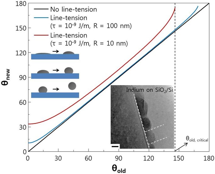
Line tension effect with respect to the diameter of liquid metal (for the case of 10 nm and 100 nm radius).
The line tension value was set as 10−9 J/m. The inset is TEM image of indium nanoparticle on SiO2/Si substrate. The contact angle between SiO2 and indium was about 90°. Scale bar, 10 nm.
-
iv
Polyimide surface: The only reference study available seems to be that of a Cu droplet on polyimide. In this study40, the interfacial energy between Cu and polyimide was calculated to be about 1.6 J/m2. Normally, the surface energy of a solid polyimide surface (σsv) is below 0.05 J/m2. In this case, cos θold ≪ −1, so θold is out of range. The polymer film prepared by spin coating and curing can have different surface properties compared to the metal and oxide surfaces studied herein. As a result, we cannot estimate the exact contact angle of liquid indium on polyimide.


Plot of the In(Sn) nanodot density as a function of the surface energy of the various substrates.
The inset shows the AFM images of In(Sn) nanodot. Scale bar, 200 nm.
Next, we considered the effect of line tension effect on θold (Fig. 5). As droplet size decreases below the nanometer range, the line tension (τ: three phase contact line) effect should be considered. Therefore, the new contact angle should be rewritten as: cos θnew = cos θold − τ/(σlvR), where R is the radius of the solid−liquid contact area41,42,43. In a vacuum, metal nanoparticles normally have θnew ≈ 10−9 N/m44. The radius of an In nanodot is ~10 nm (inset, Fig. 5). Using this information, we can draw a relation between θold and θnew. The new contact angle equation implies that θnew > θold. The critical contact angle of θold (where θnew = 180°) is ~146°. θnew of the In nanodot on SiO2 is ~90° (θold = 80°), which is similar to the value shown in the inset TEM image of Fig. 5. Moreover, the decrease of the density of the In nanodots on a sapphire surface compared to an SiO2 surface could be understood to cause the higher θnew > 145° due to the line tension effect (θold ≈ 130°, which is near the critical angle for desorption, which means that θnew = 180°). The decrease in In(Sn) nanodot density on materials with extremely low surface energy, such as polyimide, could also be understood in the context of the positive line tension effect (desorption from the surface due to high contact angle). The detailed information for the contact angle of In particles on several surfaces are summarized in table 1.
The perfect wetting and abnormal In(Sn) nanodot formation on the W surface (Fig. 6b) clearly caused difference in the nanostructure development from that on an SiO2 surface, which showed uniform nanostructure growth (Fig. 6a). A metal catalyst coated on W surface will change the surface energy of W and tends to cause formation of a large catalyst by a ripening process45, resulting in abnormal diameter distribution of ITO nanowires. Moreover, the ITO nanowires on c-plane sapphire (Fig. 6c) had much smaller diameter (~10 nm) than those on the other substrates. This phenomenon can be explained by the high contact angle of liquid In (θold ~ 130°; θnew ~ 145°) on c-sapphire. Increasing contact angle decreases the contact area with the substrate and therefore decreases the diameter of the ITO nanowires during segregation. ITO nanowires have a larger diameter (>40 nm) on a W surface than on a sapphire surface because liquid In has a lower contact angle (θold ~ 30°) on W than on sapphire. If we assume the total volume of metal particles to be constant, we can calculate the contact radius of this particle on several substrates (table 2). This calculation shows a similar tendency to that shown in the SEM image (Fig. 6). To summarize, the surface energy of the substrate effects the contact angle of the liquid droplet at the early stage of growth (from the decomposition of metal-oxide source during electron-beam irradiation) and this effect results in variation of the density and diameter of the metal-oxide nanowires formed.

SEM morphology evolution of In(Sn) oxide nanostructures with respect to growth time (a) on SiO2/Si substrate, (b) on W coated c-plane sapphire and (c) on bare c-sapphire substrate. Scale bar, 200 nm.
The distribution of In(Sn) nanodot size on the polyimide surface (inset AFM image, Fig. 4) is non-uniform compared to that on SiO2 and c-plane sapphire surfaces. To understand this phenomenon, we must consider the surface migration and agglomeration of In(Sn) nanodots. Because polyimide has very low surface energy, the metal nanoparticles on the surface could migrate easily during growth. We compared the distribution of In(Sn) nanodots on specific substrates that had similar surface energy but different surface migration energy, e.g., n-graphene substrate (Fig. 7a)22,23,24. The surface energy of n-graphene is independent of n (Fig. 7b). The surface energy distribution was determined from the contact angle using DI water and diiodomethane as the probe liquids and calculated using the geometric mean equation: (1 + cosθ)γpl = 2(γsdγpld)1/2 + 2(γspγplp)1/2, where γs and γpl are the surface energies of the sample and the probe liquid, respectively and the superscripts d and p refer to the dispersion and polar (non-dispersion) components of the surface energy, respectively46. The calculated surface energy of graphene (~46 to 47 mJ/m2) matched quite well with previous reports47. However, the surface migration energy of the graphene surface is strongly dependent on n, due to Van der Waals forces between the single graphene layers (Bernal AB stacked graphenes)22,23,24. Although the n-graphenes made by the multiple transfer process do not have perfect AB Bernal stacking order, AB stacking structures can occur over small areas due to the polycrystalline characteristics of CVD graphenes. The Raman spectrum of 1-layer graphene (Fig. 7c) shows the features of monolayer graphene: (i) a 2.0 ~ 3.0 2D/G intensity ratio and (ii) a symmetric 2D band48. All of the samples had weak D and G* bands, which is unavoidable in graphene samples grown on polycrystalline copper foil using CVD. The red-shift of the G band and unsymmetrical 2D peaks in the Raman spectrum for 2 and 3-layer graphenes indicated that the anharmonic scattering of optical phonons that are active in the Raman scattering processes increased due to the additional AB stacking graphene layers49. When grown at 300°C for 6 s, initial In(Sn) nanodot distribution was affected by the number of graphene layers, from 0 (bare SiO2 covered Si) to 3 (Fig. 7d). The strong migration tendency of single-layer graphene caused abnormal nanodot agglomeration. This migration tendency gradually disappeared as the number of graphene layers increased from 1 to 3, (schematics, Fig. 7d) due to strong Van der Waals forces between layers.

(a) Camera image of graphene transferred 3 times onto SiO2/Si(100) surfaces. Scale bar, 1 cm. (b) Contact angle of n-layer graphene using DI water and diiodomethane and calculated surface energy based on the geometric mean equation. (c) Raman spectrum of n-layer graphene. (d) Top view SEM images of In(Sn) nanodots on n-layer graphene at the early stage of growth and their schematics. The n = 0 layer is bare SiO2/Si substrate. Scale bar, 500 nm.
Considering all the experimental results, we believe that metal oxides could easily be decomposed by a high density electron-beam and that sufficient metal flux for the self-catalysis of the VLS process can be formed under a low oxygen partial pressure. Therefore, the metal oxide nanostructures synthesized by the VLS process can be achieved easily at a temperature just above the melting point of the metallic self-catalyst. In this synthesis process, the surface energy and surface migration energy of the substrate strongly effects the density of the self-catalyst distribution and the final morphology of the nanostructures. The density of the self-catalytic nanodots increased with decreasing surface energy of the substrate, due to the perfect wetting of catalytic materials on high surface energy substrates. However, surfaces with extremely low surface energy have difficulty producing self-catalytic nanodots with high density, due to positive line tension which increases the contact angle > 180°. Moreover, substrates with low surface migration energy, such as single layer graphene, cause the nanodots to agglomerate, thereby producing a non-uniform distribution compared to substrates with high surface migration energy.
Conclusion
We studied the growth mechanism of metal oxide nanostructures by the simple electron beam evaporation. The high density of the electron beam can easily decompose metal oxides that have high melting points. The decomposed metal elements form the self-catalysts for the VLS process and the metal oxide nanostructure can be grown at a temperature just above the melting point of the metal. The morphology of the nanostructures, such as density and uniformity, is strongly dependent on the surface energy and surface migration energy of the substrate. Due to its simplicity and scalability, this method to fabricate metal oxide nanostructures could have applications in many fields, such as energy and environmental science, electronics, photonics and biology.
Methods
Electron beam evaporation
The group 13 metal oxide nanostructures (Al2O3, Ga2O3 and Sn 10% doped In2O3) were fabricated by the electron beam evaporation method using high purity (99.99%) oxide pellets as the source materials50,51. The nanostructures were grown at a rate of 0.5 nm s−1 and the chamber pressure was maintained at approximately 10−5 Torr during deposition. The substrate temperature was controlled using a heating element made by SiC and calibrated by k-type thermocouple. Substrate preparation: Several substrates with different surface energies were prepared; Si(100) covered by thermal oxide at about 200 nm, c-plane sapphire, tungsten film (50 nm) coated by magnetron sputtering (3 mTorr argon plasma, 100 Watt RF power, 300°C) on c-plane sapphire and spin-coated polyimide film (cured at 150°C) on soda-lime glass. Substrates were prepared and cleaned sequentially with acetone, ethyl-alcohol and de-ionized water. For the n-layer graphene substrates, the conventional chemical vapor deposition (CVD) method using copper foil as a catalyst was used52,53. The copper foils (Alfa Aesar, item No. 13382, 99.8% purity) were loaded into the quartz tube reaction chamber. A typical growth process was conducted as follows: (1) the pressure in the growth chamber was pumped down to 5 mTorr using a mechanical pump; (2) a 40 sccm flow of hydrogen gas was introduced into the chamber at 950 mTorr; (3) a the copper foils were heated to 1000°C for 60 min and annealed for 30 min to enlarge the copper grains and remove residual copper oxide and impurities; (4) a 6 sccm flow of methane gas with 20 sccm hydrogen was introduced into the chamber for 10 min with a total pressure of 420 mTorr for graphene synthesis; (5) after growth, the furnace was cooled rapidly to RT under a 20 sccm flow of hydrogen. The synthesize graphenes were transferred onto SiO2/Si(100) substrate 3 times to make n-layer graphene surfaces. First, one side of the graphene/copper foils were spin coated with polymethyl methacrylate (PMMA) and dried in atmosphere. Then, the uncoated graphenes were etched with oxygen plasma for 30 sec at 100 W. After the copper foils were totally etched in (NH4)2S2O8 solution (0.1 M) for 12 hours, the graphene/PMMA films were washed in DI water several times. The graphene/PMMA films were transferred onto SiO2/Si(100) substrate and dried at ambient temperature, then heated at 180°C for 30 min. Finally, the PMMA layers were removed with acetone. Analysis: Scanning electron microscopy (SEM) with a PHILIPS XL30S was carried out at an acceleration voltage of 10 kV and working distance of 5 mm. For the elemental analysis at the initial stage of growth, the electron energy loss spectroscopy (EELS) map attached function in high-resolution transmission electron microscopy (HRTEM: model Cs-corrected JEM2200FS operated at 200 kV) was carried out. Atomic force microscopy (AFM) images were recorded using a Digital Instruments Nanoscope in tapping mode with silicon cantilevers. The Raman spectrum was obtained with a Raman spectrometer LabRAM HR 800 from the company HORIBA Yvon GmbH under the following conditions: excitation wavelength of the laser: He-Ne 633 nm; spot size of the laser beam: 5 μm in diameter; measurement time: 10 sec.
References
Poizot, P., Laruelle, S., Grugeon, S., Dupont, L. & Tarascon, J.-M. Nano-sized transition-metal oxides as negative-electrode materials for lithium-ion batteries. Nature 407, 496–499 (2000).
Qin, Y., Wang, X. & Wang, Z. L. Microfibre–nanowire hybrid structure for energy scavenging. Nature 451, 809–813 (2008).
Nam, K. T. et al. Virus-enabled synthesis and assembly of nanowires for lithium ion battery electrodes. Science 312, 885–888 (2006).
Xi, J.-Q. et al. Optical thin-film materials with low refractive index for broad-band elimination of Fresnel reflection. Nat. Photonics 1, 176–179 (2007).
Xie, X., Li, Y., Liu, Z.-Q., Hatuta, M. & Shen, W. Low-temperature oxidation of CO catalysed by Co3O4 nanorods. Nature 458, 746–749 (2007).
Wagner, R. S. & Ellis, W. C. Vapor-liquid-solid mechanism of single crystal growth. Appl. Phys. Lett. 4, 89–90 (1964).
Park, W. I., Kim, D. H., Jung, S.-W. & Yi, G.-C. Metalorganic vapor-phase epitaxial growth of vertically well-aligned ZnO nanorods. Appl. Phys. Lett. 80, 4232–4234 (2002).
Kolasinski, K. W. Catalytic growth of nanowires: Vapor–liquid–solid, vapor–solid–solid, solution–liquid–solid and solid–liquid–solid growth. Curr. Opin. Solid State Mater. Sci. 10, 182–191 (2006).
Mohammad, S. N. Self-catalysis: A contamination-free, substrate-free growth mechanism for single-crystal nanowire and nanotube growth by chemical vapor deposition. J. Chem. Phys. 125, 094705 (2006).
Mohammad, S. N. Analysis of the vapor–liquid–solid mechanism for nanowire growth and a model for this mechanism. Nano. Lett. 8, 1532–1538 (2008).
Hu, J. Q., Bando, Y. & Golberg, D. Self-catalyst growth and optical properties of novel SnO2 fishbone-like nanoribbons. Chem. Phys. Lett. 372, 758–762 (2003).
Han, X. et al. Controllable synthesis and optical properties of novel ZnO cone arrays via vapor transport at low temperature. J. Phys. Chem. B 109, 2733–2738 (2005).
Xue, X. Y. et al. Synthesis and ethanol sensing properties of indium-doped tin oxide nanowires. Appl. Phys. Lett. 88, 201907 (2006).
Chiquito, A. J., Lanfredi, A. J. C. & Leite, E. R. One-dimensional character of Sn doped In2O3 nanowires probed by magnetotransport measurements. J. Phys. D: Appl. Phys. 41, 045106 (2008).
Hoffmann, S. et al. Axial p-n junctions realized in silicon nanowires by ion implantation. Nano Lett. 9, 1341–1344 (2009).
Kumar, R. R., Rao, K. N., Rajanna, K. & Phani, A. R. Low temperature growth of SnO2 nanowires by electron beam evaporation and their application in UV light detection. Mater. Res. Bull. 48, 1545–1552 (2013).
Kumar, R. R., Yuvaraj, D. & Rao, K. N. Growth and characterization of germanium nanowires by electron beam evaporation. Mater. Lett. 64, 1766–1768 (2010).
Kumar, R. R., Rao, K. N. & Phani, A. R. Growth of silicon nanowires by electron beam evaporation using indium catalyst. Mater. Lett. 66, 110–112 (2012).
Kumar, R. R., Rao, K. N. & Phani, A. R. Bismuth catalyzed growth of silicon nanowires by electron beam evaporation. Mater. Lett. 82, 163–166 (2012).
Ohya, Y., Yamamoto, T. & Ban, T. Equilibrium dependence of the conductivity of pure and tin-doped indium oxide on oxygen partial pressure and formation of an intrinsic defect cluster. J. Am. Ceram. Soc. 91, 240–245 (2008).
Yu, H. K., Dong, W. J., Jung, G. H. & Lee, J.-L. Three-dimensional nanobranched indium-tin-oxide anode for organic solar cells. ACS nano 5, 8026–8032 (2011).
Zhou, H. et al. Thickness-dependent morphologies of gold on n-layer graphenes. J. Am. Chem. Soc. 132, 944–946 (2010).
Luo, Z. et al. Size-selective nanoparticle growth on few-layer graphene films. Nano Lett. 10, 777–781 (2010).
Zhou, H. et al. Thickness-dependent morphologies and surface-enhanced Raman scattering of Ag deposited on n-layer graphenes. J. Phys. Chem. C 115, 11348–11354 (2011).
Allen, G. L., Bayles, R. A., Gile, W. W. & Jesser, W. A. Small particle melting of pure metals. Thin Solid Film 144, 297–308 (1986).
Xie, D. et al. Thermal stability of indium nanocrystals: A theoretical study. Mater. Chem. Phys. 96, 418–421 (2006).
Gao, J. et al. Phase selection enabled formation of abrupt axial heterojunctions in branched oxide nanowires. Nano Lett. 12, 275–280 (2012).
Meng, G. et al. Impact of preferential indium nucleation on electrical conductivity of vapor−liquid−solid grown indium−tin oxide nanowires. J. Am. Chem. Soc. 135, 7033–7038 (2013).
Beaudry, A. L., Tucker, R. T., LaForge, J. M., Taschuk, M. T. & Brett, M. J. Indium tin oxide nanowhisker morphology control by vapour–liquid–solid glancing angle deposition. Nanotechnology 23, 105608 (2012).
Liang, C., Meng, G., Lei, Y., Philipp, F. & Zhang, L. Catalytic growth of semiconducting In2O3 nanofibers. Adv. Mater. 13, 1330–1333 (2001).
Barin, I. Thermochemical data of pure substances [716–717] (Wiley, New York, 1989).
Yang, S. Y. et al. Enhanced electrical percolation due to interconnection of three-dimensional pentacene islands in thin films on low surface energy polyimide gate dielectrics. J. Phys. Chem. B 110, 20302–20307 (2006).
Danielson, D. T., Sparacin, D. K., Michel, J. & Kimerling, L. C. Surface-energy-driven dewetting theory of silicon-on-insulator agglomeration. J. Appl. Phys. 100, 083507 (2006).
Guo, J., Ellis, D. E. & Lam, D. J. First-principles calculation of the electronic structure of sapphire: Bulk states. Phys. Rev. B 45, 3204–3214 (1992).
Fu, C. L., Ohnishi, S., Jansen, H. J. F. & Freeman, A. J. All-electron local-density determination of the surface energy of transition metals: W(001) and V(001). Phys. Rev. B 31, 1168–1171 (1985).
Aldrich, R. G. & Keller, D. V., Jr. Investigation of the contact angle between indium (I) and an aluminum substrate in ultrahigh vacuum. J. Appl. Phys. 36, 3546–3548 (1965).
Senkara, J. & Wlosinski, W. K. Surface phenomena at the interfaces of the tungsten-liquid Cu-Sb alloy system. J. Mater. Sci. 20, 3597–3604 (1985).
Nikolopoulos, P., Sotiropoulou, D. & Ondracek, G. Temperature-dependence of interfacial energies between solid oxide ceramics and liquid metals. J. Therm. Anal. 33, 633–642 (1988).
Bettge, M. et al. Importance of line and interfacial energies during VLS growth of finely stranded silica nanowires. J. Mater. Res. 26, 2247–2253 (2011).
Menezes, M., Robertson, I. M. & Birnbaum, H. K. Measurement and improvement of the adhesion of copper to polyimide. J. Mater. Res. 14, 4025–4034 (1999).
Raspal, V. et al. Nanoporous surface wetting behavior: The line tension influence. Langmuir 28, 11064–11071 (2012).
Gretz, R. D. Line-tension effect in a surface energy model of a cap-shaped condensed phase. J. Chem. Phys. 45, 3160–3161 (1966).
Weijs, J. H., Marchand, A., Andreotti, B., Lohse, D. & Snoeijer, J. H. Origin of line tension for a Lennard-Jones nanodroplet. Phys. Fluids 23, 022001 (2011).
Sutter Eli, A. & Sutter, P. W. Size-dependent phase diagram of nanoscale alloy drops used in vapor-liquid-solid growth of semiconductor nanowires. ACS nano 4, 4943–4947 (2010).
Guo, D. L. et al. Metal-layer-assisted coalescence of Au nanoparticles and its effect on diameter control in vapor-liquid-solid growth of oxide nanowires. Phys. Rev. B 83, 045403 (2011).
Owens, D. K. & Wendt, R. C. Estimation of the surface free energy of polymers. J. Appl. Polym. Sci. 13, 1741–1747 (1969).
Wang, S., Zhang, Y., Abidi, N. & Cabrales, L. Wettability and surface free energy of graphene films. Langmuir 25, 11078–11081 (2009).
Ferrari, A. C. et al. Raman spectrum of graphene and graphene layers. Phys. Rev. Lett. 97, 187401 (2006).
Chen, S. et al. Raman measurements of thermal transport in suspended monolayer graphene of variable sizes in vacuum and gaseous environments. ACS Nano 5, 321–328 (2011).
Yu, H. K. et al. Nano-branched transparent conducting oxide: Beyond the brittleness limit for the flexible electrode applications. Nanoscale 4, 6831–6834 (2012).
Yu, H. K. & Lee, J.-L. Effect of ion beam assisted deposition on the growth of indium-tin-oxide (ITO) nanowires. CrystEngComm. 16, 4108–4112 (2014).
Gulde, M. et al. Ultrafast low-energy electron diffraction in transmission resolves polymer/graphene superstructure dynamics. Science 345, 200–204 (2014).
Yu, H. K. et al. Chemical vapor deposition of graphene grown on “peeled-off” epitaxial Cu(111) foil: A simple approach to improved properties. ACS nano 8, 8636–8643 (2014).
Acknowledgements
This work was supported in part by the Priority Research Centers Program through the National Research Foundation of Korea (NRF) funded by the Ministry of Education, Science and Technology (2010-0029711) and in part by the WCU (World Class University) program through the Korea Science and Engineering Foundation, funded by the Ministry of Education, Science and Technology (Project No. R31-2008-000-10059-0).
Author information
Authors and Affiliations
Contributions
H.K.Y. performed the experiments and analyzed the data. H.K.Y. and J.–L.L. discussed the results and commented on the manuscript. J.–L.L. conceived of and supervised this study and provided intellectual and technical guidance.
Ethics declarations
Competing interests
The authors declare no competing financial interests.
Electronic supplementary material
Supplementary Information
Supplementary information for publication
Rights and permissions
This work is licensed under a Creative Commons Attribution 4.0 International License. The images or other third party material in this article are included in the article's Creative Commons license, unless indicated otherwise in the credit line; if the material is not included under the Creative Commons license, users will need to obtain permission from the license holder in order to reproduce the material. To view a copy of this license, visit http://creativecommons.org/licenses/by/4.0/
About this article

Cite this article
Yu, H., Lee, JL. Growth mechanism of metal-oxide nanowires synthesized by electron beam evaporation: A self-catalytic vapor-liquid-solid process. Sci Rep 4, 6589 (2014). https://doi.org/10.1038/srep06589
Received:
Accepted:
Published:
DOI: https://doi.org/10.1038/srep06589
- Springer Nature Limited
This article is cited by
-
Review: Oxygen-deficient tungsten oxides
Journal of Materials Science (2021)
-
Enhanced black state induced by spatial silver nanoparticles in an electrochromic device
NPG Asia Materials (2017)